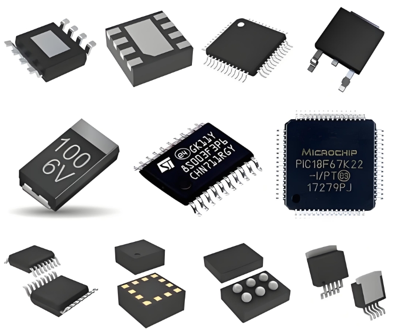
Intel DT28F160S375: A Technical Overview of a 16Mbit SmartVoltage Boot Block Flash Memory
The Intel DT28F160S375 represents a significant advancement in the architecture of non-volatile memory solutions, specifically engineered for systems requiring reliable firmware storage and in-circuit programmability. As a 16-megabit (2M x 8/1M x 16) boot block Flash memory device, it incorporates several key technologies that made it a cornerstone for embedded designs in computing, telecommunications, and industrial applications.
A defining characteristic of this memory IC is its SmartVoltage technology, which provides unparalleled flexibility in system design. The device can operate across three voltage ranges: a 12.0V VPP for accelerated programming, a 5.0V VCC for standard read operations, and a 3.3V VCC for low-power read operations. This multi-voltage capability allows the same device to be used in mixed-voltage systems, reducing component count and simplifying power supply design.
The memory array is organized using the Boot Block architecture, a critical feature for modern firmware storage. This architecture partitions the memory into multiple blocks with asymmetric sizes. It features:
One 16-Kbyte boot block at the top or bottom of the address space, which can be locked to prevent accidental corruption of the primary boot code.
Two parameter blocks (8 Kbytes each).

One main block (96 Kbytes).
Additional uniform blocks filling the remainder.
This structure protects critical code while allowing other memory sections to be updated for firmware revisions or data storage.
For in-system programming and erasure, the DT28F160S375 complies with the JEDEC-standard pinout and command set, ensuring compatibility with industry-standard programming algorithms. It offers a fast word-programming time of 10 µs and a block-erase time of approximately one second. The device also features an erase suspend/resume function, allowing the system to halt an erase operation to read data from another block, thus enhancing overall system efficiency.
Furthermore, the device includes hardware and software data protection mechanisms. The Write Protect (WP) pin provides hardware-level protection for the two outermost boot blocks. A built-in program/erase controller automates the complex timing algorithms, minimizing overhead on the system's microprocessor.
ICGOOODFIND: The Intel DT28F160S375 is a sophisticated memory solution that masterfully combines multi-voltage operation, secure boot block architecture, and high-performance in-system reprogrammability. Its design addresses the core requirements of reliability, flexibility, and security essential for critical system firmware, making it a notable component in the evolution of Flash memory technology.
Keywords: Boot Block Architecture, SmartVoltage Technology, In-System Programmability, Non-Volatile Memory, Firmware Storage
